Table of Contents
Overview
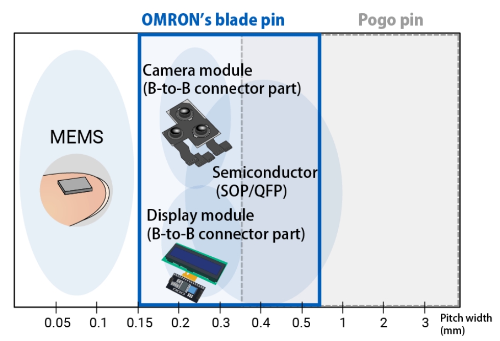
Ultra-compact electronic components are now used in various applications that support the foundation of our lives, such as smartphones, car navigation systems, and advanced driving technology. Naturally, there are various shapes of sockets used in the inspection equipment for these components. Applications that support social infrastructure such as smartphones have a fast release cycle for new products, so the socket shape on the inspection side changes each time. Inspection equipment for electronic components requires not only technical capabilities to respond to the speed, but also high measurement accuracy to accurately check the performance of extremely small electronic components and a narrow pitch to accommodate increasingly high-density products.
![[Customer’s final product] Short-term release cycle: The shape of the camera varies depending on the smartphone. It changes every time a new product comes out. [Inspection equipment] Short-term specification change [Inspection socket / pin] Short-term shape change: The shape is customized to suit the device under test (DUT) at a design speed that can correspond to the release cycle. => Speed design, high precision, and narrow pitch products are required.](/eu-en/sites/components.omron.com.eu/files/2023-05/efc-top_01_01_en.jpg)
Four values of OMRON’s probe pin

OMRON’s testing sockets use probe pins manufactured using its proprietary* electro formed components (EFC) process technology. Highly durable pins with complex shapes and excellent spring property that are difficult to fabricate by metal bending or other processing can be manufactured with precision on the order of microns. With our EFC process technology and many years of know-how, we propose sockets with a shape suitable for the customer’s device under test (DUT) with the same design speed as that of pogo pin products while achieving better inspection characteristics than pogo pin products. OMRON’s testing sockets boasting high durability (long operating life) and high precision contribute greatly to the reduction of maintenance man-hours for customers. In addition, OMRON’s plate-shaped probe pins excel at pin placement with narrow pitch spacing for the inspection of high-performance, high-density products.
Contact OMRON with your concerns and consultation regarding the inspection of extremely small electronic components.
*Two patents (US8337261; US2013/0045617) have been granted for the electroforming technology to form the contact structure and its manufacturing process.
Please refer to the video below for a detailed overview.
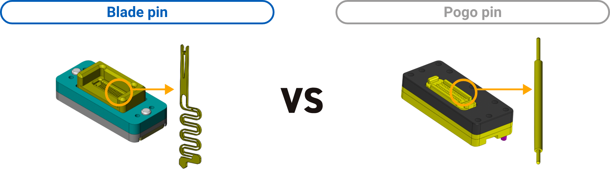
Pogo Pin and OMRON’s Probe Pin (Blade Pin)
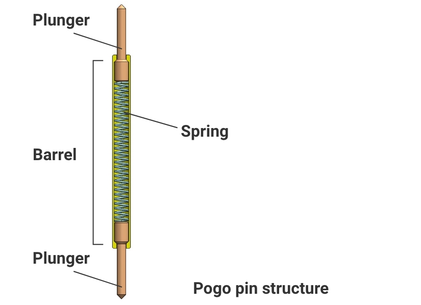
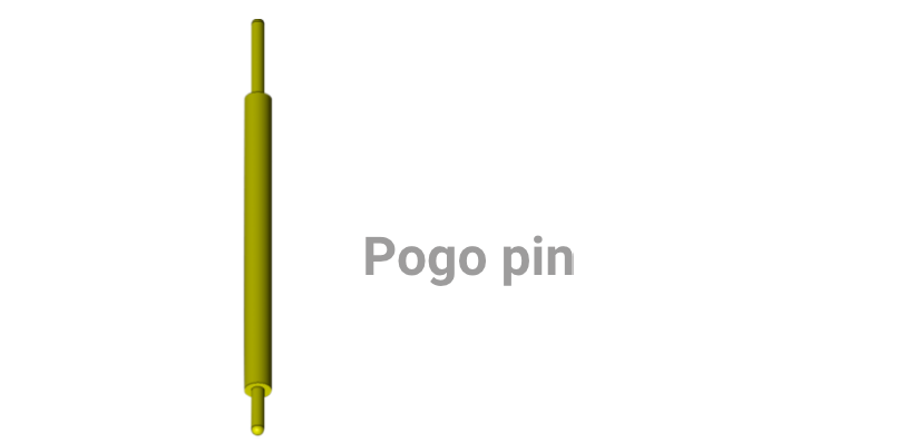
What is Pogo Pin?
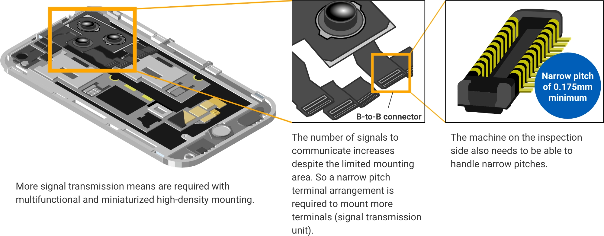
In general, IC testing sockets are equipped with an extendable rod-shaped probe pin (inspection pin) called a pogo pin, which is used as a part to electrically connect the PC board on the inspection equipment side and the DUT. The pogo pin consists of three main parts: plunger, barrel, and spring. The pogo pin is also called a probe pin, spring probe, or contact probe. However, with the acceleration of miniaturization, multi-functionality, and high-density mounting of device, inspection needs that are difficult to meet with the pogo pin, such as high inspection stability, long operating life, narrow pitch, and low contact resistance, are becoming more apparent.
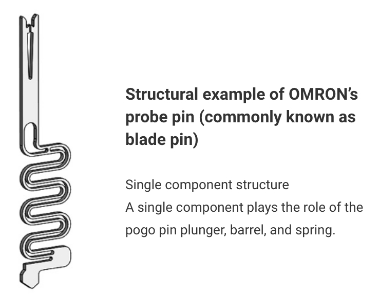
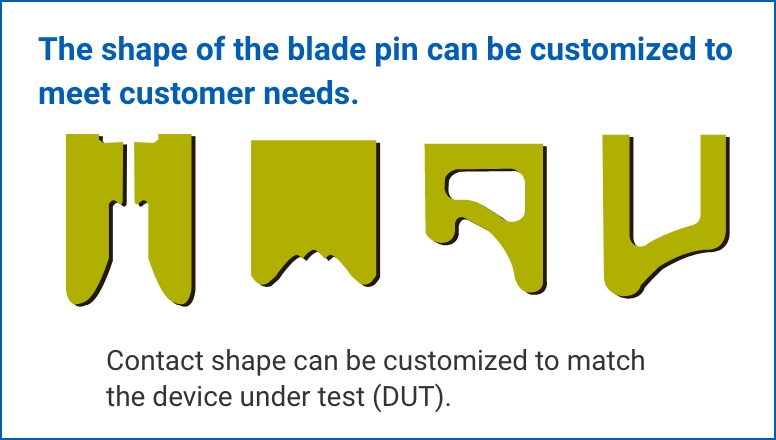
What is OMRON’s probe pin (blade pin)?
OMRON’s testing sockets use a probe pin (commonly known as a blade pin) manufactured using OMRON’s proprietary*1 EFC process technology. The blade pin has a completely different structure from the pogo pin and is characterized by its ability to reproduce a complex pin shape in a single component structure. OMRON can custom design and propose the contact shape suitable for the device under test (DUT). OMRON’s probe pins use original materials*2 with excellent hardness and spring property. The probe pins outperform pogo pins with four key advantages: high durability, low contact resistance, high inspection pass rate, and narrow pitch.
*1 Two patents (US8337261; US2013/0045617) have been granted for the electroforming technology to form the contact structure and its manufacturing process.
*2 Patent No. 5077479
Comparison of OMRON’s probe pin (blade pin) and pogo pin
| Over 500,000 times |  |
Less than 100,000 times |
| 30mΩ High inspection accuracy even for devices under test that require low contact resistance |
 |
70mΩ Difficult to use for devices under test that require low contact resistance |
| 99 to 100% |  |
80 to 99% |
| 0.20mm or less |  |
0.35mm or more |
*An example of B-to-B connector inspection
Four Values Provided by the Blade Pin

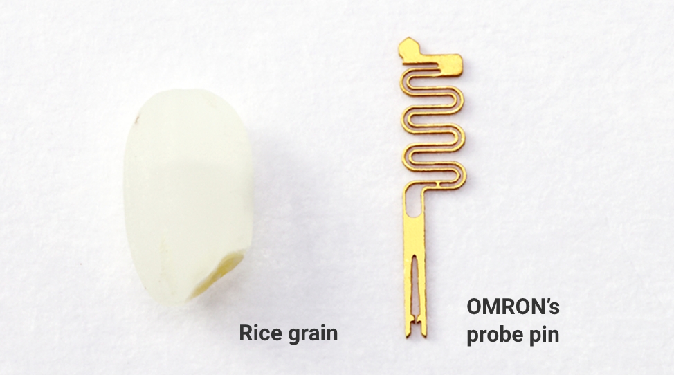
Because the testing pin used for the inspection of small components such as semiconductors is very thin, with a diameter of 1 mm or less, durability is an issue. The number of times semiconductor components that are part of our daily lives are inspected ranges from tens of thousands to hundreds of thousands of times per day. Therefore, if the pin durability is low, 100 to 10,000 pins on the inspection equipment must be replaced daily, depending on the inspection requirements of the device under test (DUT). The mechanical durability of OMRON’s testing pins is over 500,000 times, approximately five times more than that of pogo pins.
OMRON’s blade pins help customers reduce maintenance man-hours and improve production efficiency.
 |
 |
|
| Site | Maintenance-free and in constant operation 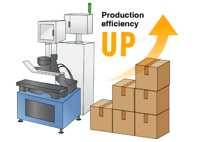 Long pin operating life improves production efficiency. |
Need to stop operation for regular maintenance.  100 to 10,000 pins must be replaced daily, depending on the device under test. |
|---|---|---|
| Mechanical durability | *Over 500,000 times | *Less than 100,000 times |
*An example of B-to-B connector inspection
OMRON’s EFC process technology enables long operating life
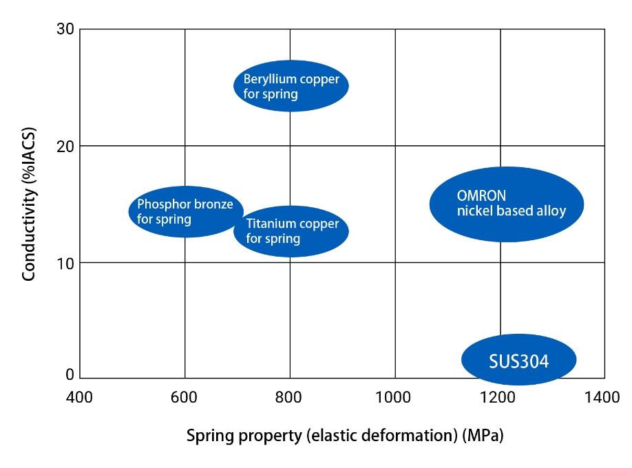
OMRON’s original material blend provides excellent spring property and conductivity
By using OMRON’s original materials that can only be used with the EFC process technology, it is possible to process pins with mechanical properties equivalent to SUS304 and electrical properties equivalent to copper alloys.
*Patent No. 5077479

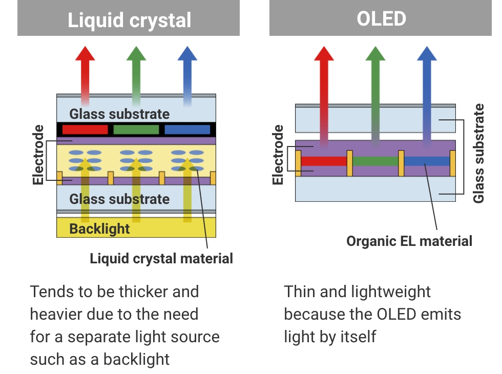
Displays for computers, televisions, smartphones, and other devices are evolving rapidly. With the emergence of products that are clearer and more sensitive to operation, OLEDs (organic light emitting diodes) are gaining attention. Liquid crystals, which are often used as conventional displays, do not emit light by themselves and require a separate light source. However, OLEDs, which are LEDs using an organic substance as the light-emitting material, emit light spontaneously when electric current is applied, so they do not require a separate light source. Therefore, it is possible to configure very thin and light displays that meet today’s display needs.
Although OLEDs have such high advantages, it is difficult to inspect the electrical characteristics of their application. Since the internal resistance of OLEDs is very low, if the resistance on the testing socket side is high, luminance inspection cannot be performed because sufficient current is not ensured to make OLEDs emit light.
The lower the resistance on the inspection equipment side, the more accurate performance inspection can be performed on the application side. OMRON’s probe pins (blade pins) have a low contact resistance of 30mΩ, which is less than half that of pogo pins, and do not interfere with device inspection. They enable highly accurate and smooth inspection.
|
|
|
| Site | Inspectable 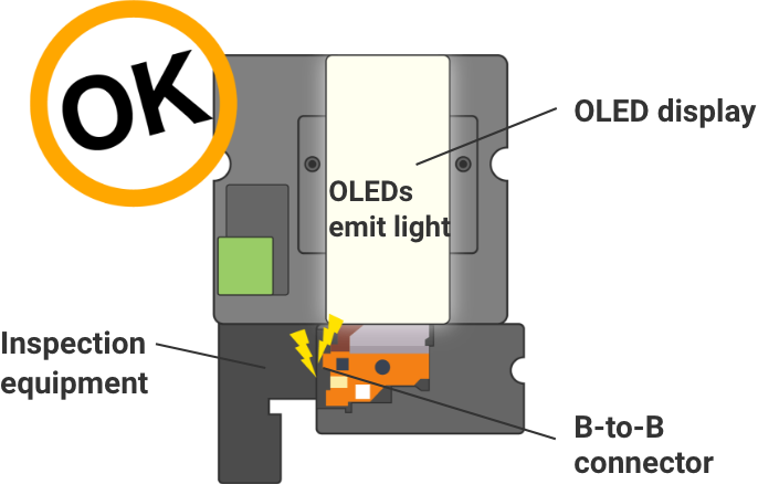 Due to low contact resistance on the inspection device side, correct inspection is possible even for products with low internal resistance, such as OLEDs. |
Un-inspectable 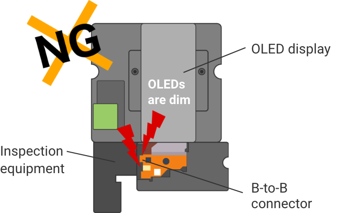 Even if the product itself has the performance to pass the test, correct inspection cannot be performed due to high contact resistance on the inspection equipment side. |
|---|---|---|
| Contact resistance | *30mΩ | *70mΩ |
*An example of B-to-B connector inspection
OMRON’s EFC process technology enables low contact resistance
![[Example] Smartphone camera module](/eu-en/sites/components.omron.com.eu/files/2023-05/efc-top_03_11_en.jpg)
Surface contact design significantly reduces resistance
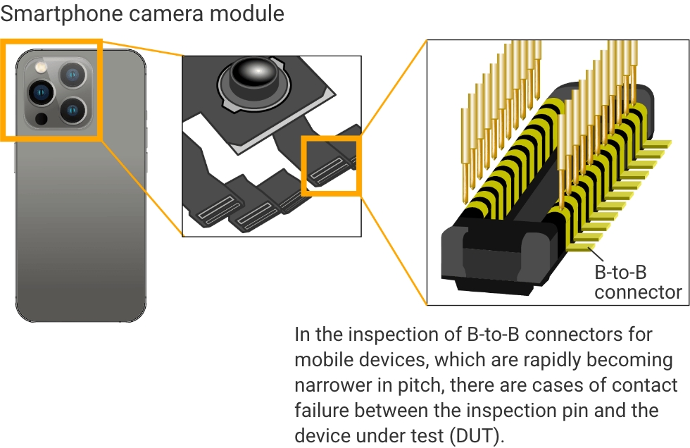
For example, the B-to-B connector used in camera modules is shaped with the conductive part of the terminal raised. When the testing pin is applied to a product with such a terminal shape, pogo pins are designed for “point contact,” it is difficult to maintain stable mechanical contact because pogo pins are designed for “point contact.” As a result, it is difficult to perform stable inspections both mechanically and electrically.
However, with OMRON’s EFC process technology, it is possible to customize blade pins shaped to suit the customer’s application. The “surface contact” design ensures reliable contact.
![[Surface contact] Blade pin / B-to-B connector](/eu-en/sites/components.omron.com.eu/files/2023-05/efc-top_03_12_en.jpg)
Blade pin
Low contact resistance due to large contact area between the blade pin and the conductive part of the connector
![[Point contact] Pogo pin / B-to-B connector](/eu-en/sites/components.omron.com.eu/files/2023-05/efc-top_03_13_en.jpg)
Pogo pin
High contact resistance due to small contact area between the blade pin and the conductive part of the connector

OMRON’s blade pins have an extremely high inspection pass rate of 99 to100%. Less than 1% of products are rejected due to testing pin contact failures, which contributes to the reduction of customers’ product disposal losses and allows inspections to be carried out with high production efficiency. The high inspection pass rate also benefits defect analysis. Defect analysis of products is one of the important factors for creating better new products. However, if there are many rejected items due to reasons on the inspection equipment side, it is not possible to correctly analyze what is the cause of the defect. OMRON’s blade pins virtually eliminate rejects due to contact failure between the testing pin and the terminal of the device under test (DUT). By reducing the defect factors caused by the inspection equipment as much as possible, more accurate product defect analysis results can be properly reflected in the product.
|
|
|
| Site | Measures the specifications of the customer’s product accurately 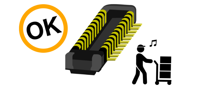 Reduces disposal loss and facilitates identification of defective areas |
Due to contact failure of the judgment testing pin, even a product that satisfies the specifications will be judged to be defective in the inspection. 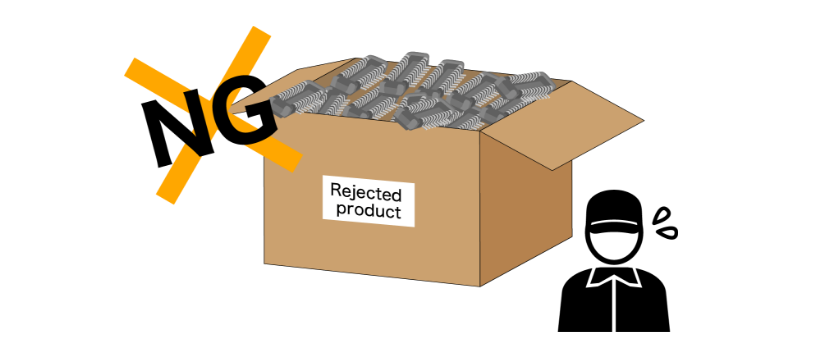 Disposal losses occur and identification of the cause of defect is difficult. |
|---|---|---|
| Inspection pass rate | *99~100% | *80~99% |
*An example of B-to-B connector inspection
OMRON’s EFC process technology enables a high inspection pass rate
Surface contact design significantly reduces contact failures
For example, the B-to-B connector used in camera modules is shaped with the conductive part of the terminal raised. When the testing pin is applied to a product with such a terminal shape, contact failure is more likely to occur because pogo pins are designed for “point contact.” However, with OMRON’s EFC process technology, it is possible to customize blade pins shaped to suit the customer’s application. The “surface contact” design ensures reliable contact.
![[Surface contact]](/eu-en/sites/components.omron.com.eu/files/2023-05/efc-top_03_18_en.jpg)
Blade pin
Possible to realize mechanically and electrically stable contact with virtually no contact failures due to surface contact between the blade pin and the conductive part.
![[Point contact] B-to-B connector](/eu-en/sites/components.omron.com.eu/files/2023-05/efc-top_03_19_en.jpg)
Pogo pin
Difficult to conduct mechanically and electrically stable inspections due to point contact between the pogo pin and the connector conductive part.
Prone to contact failure.

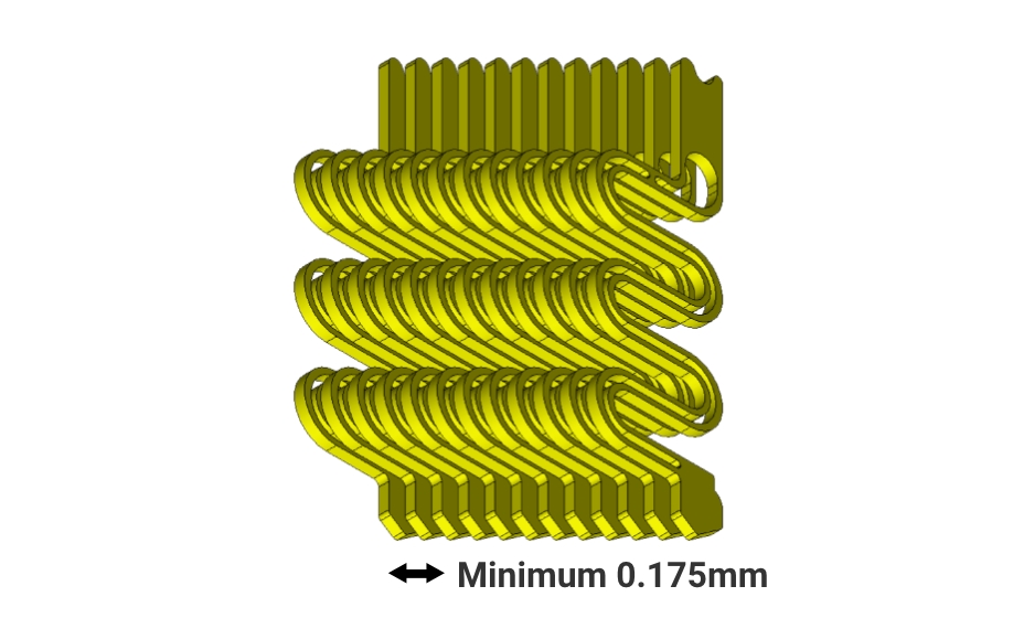
OMRON can provide testing pins for a pitch width of 0.35mm or less which is difficult to achieve with pogo pins. OMRON’s blade pins can handle a narrow pitch down to 0.175mm, enabling highly accurate inspection even for camera and display modules which are becoming increasingly multifunctional due to high-density mounting. Please feel free to contact us.
Smartphone camera module
|
|
|
| Site | Even devices under test for which high density mounting is progressing can be inspected accurately.  Plate-shaped devices under test with narrow terminal width can also be inspected. |
Unable to inspect ultra-small electronic components 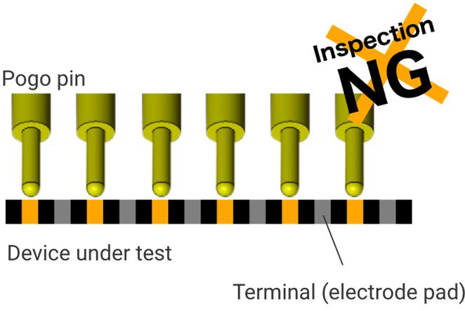 Cubic pin shape taking up a wide width. |
|---|---|---|
| Specification | *Minimum 0.175mm pitch | *Minimum 0.35mm pitch |
*An example of B-to-B connector inspection
OMRON’s EFC process technology enables narrow pitch support
EFC process technology
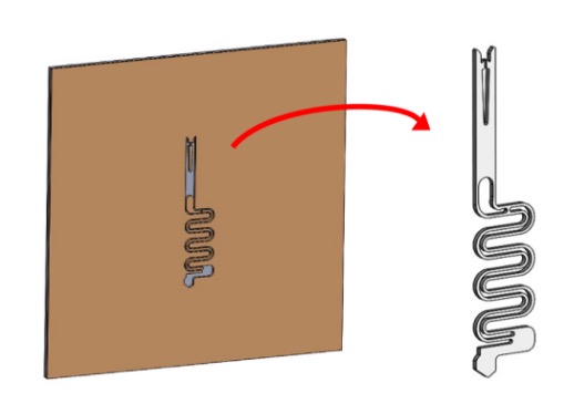
Method of depositing metal on a mold plate
OMRON’s blade pins, which are formed by depositing metal onto a mold plate using the EFC process technology, are plate-shaped and can be used side-by-side at a narrow pitch. On the other hand, pogo pins are cylindrical in shape and occupy more mounting space than plate-shaped blade pins, so it is difficult to use pogo pins with the same pitch width as blade pins.
Blade pin
Plate shape enables narrower pitches.
Minimum pitch width of 0.175mm

Pogo pin
Cylindrical shape makes it difficult to narrow the pitch compared to plate-shaped blade pins.
Minimum pitch width of 0.35mm


Width comparison between blade pin and pogo pin
Left: OMRON’s blade pin
Right: Pogo pin
Plate blade pins are thinner than cylindrical pogo pins
OMRON’s Testing Sockets
OMRON’s testing sockets are used in the final inspection of the semiconductor manufacturing process and play an important role in connecting the inspection equipment and the device under test (DUT). OMRON offers a wide range of socket types to meet customer requirements. We customize the type suitable for customer’s device under test with the optimum shape and provide it in a short delivery time.
![[Narrow pitch compatible]The world’s smallest class* of 0.175mm. (*According to our own research in March 2023) Click here for details](/eu-en/sites/components.omron.com.eu/files/2023-05/efc-top_04_01_en.jpg)
![[Automotive ECU compatible]High durability & high freedom design for reliable contact. Click here for details](/eu-en/sites/components.omron.com.eu/files/2025-02/efc-top_04_02_en.jpg)
![[High frequency compatible]Handling high frequencies up to 43.5GHz. Click here for details](/eu-en/sites/components.omron.com.eu/files/2025-02/efc-top_04_03_en.jpg)
![[High current compatible]Handling high current of 10A DC compatible with Kelvin at narrow pitches. Click here for details](/eu-en/sites/components.omron.com.eu/files/2025-02/efc-top_04_04_en.jpg)
![[High hardness compatible]Outstanding durability greatly reduces pin replacement frequency. Click here for details](/eu-en/sites/components.omron.com.eu/files/2025-02/efc-top_04_05_en.jpg)
![[SOP compatible]Accurately measurable without damaging small products. Click here for details](/eu-en/sites/components.omron.com.eu/files/2025-02/efc-top_04_06_en.jpg)
![[High temperature compatible]Operable in high temperature environments up to 200°C. Click here for details](/eu-en/sites/components.omron.com.eu/files/2025-02/efc-top_04_07_en.jpg)
OMRON’s EFC Process Technology
(Electroforming Microfabrication Technology)
OMRON’s testing sockets and pins for extremely small electronic components are created by combining EFC process technology and extensive know-how in electronic component design. Our EFC process technology is a type of electroforming microfabrication technology. This technology makes it possible to reproduce high-precision, complex shape processing in an extremely small size which was difficult to achieve with conventional press working, etc.
The EFC process technology provides customers with four values that are difficult to achieve with other technologies.
Four values only EFC process technology can realize