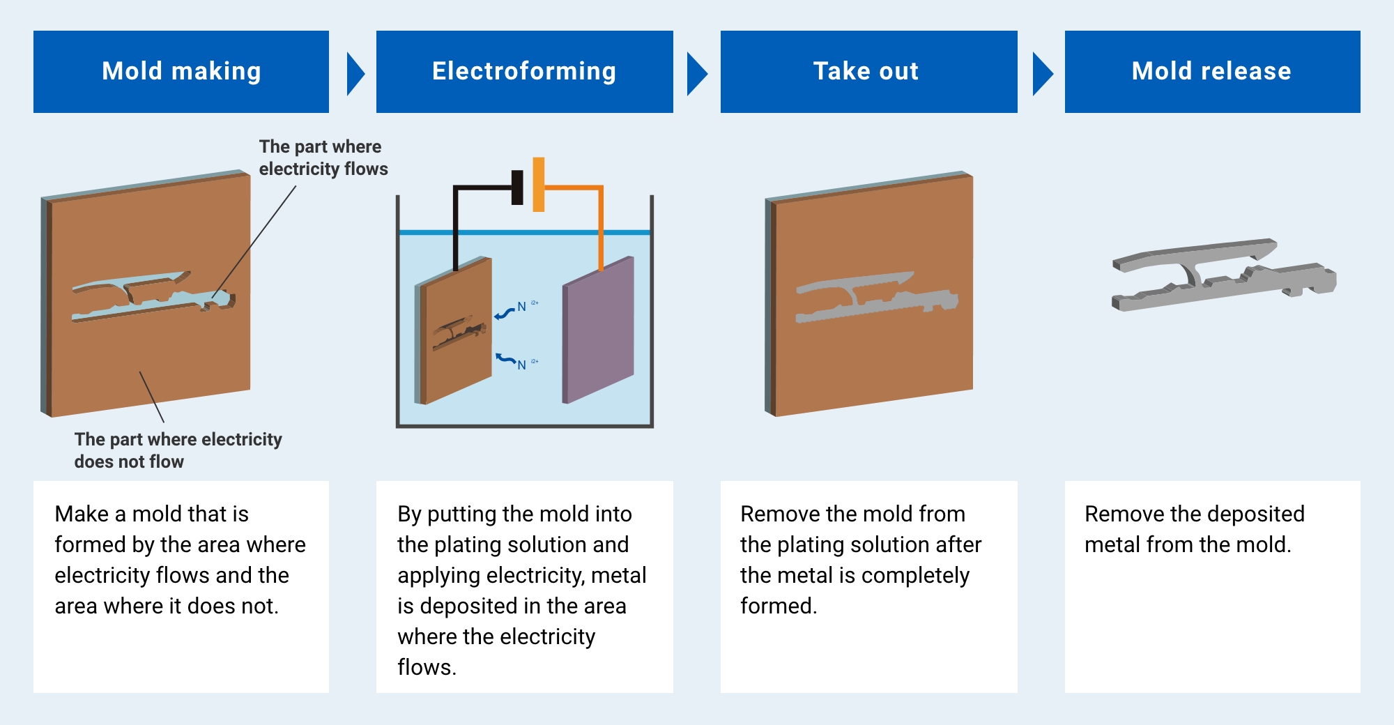
OMRON’s EFC process technology (electroforming microfabrication technology)
OMRON’s EFC process technology is a type of electroforming microfabrication technology. It is possible to reproduce highly precise and complex shapes in an extremely small size which has been difficult with conventional press work. Lithography-based mold making enables highly reproducible and accurate fabrication down to the submicron level.

Press working, etching processing, and wire cutting usually result in a rough cross section, making it difficult to achieve a smooth surface finish. If the Ra (surface roughness) of the testing pin is high, the testing pin will damage the product, leading to poor contact and product damage. However, OMRON’s EFC process technology can produce smooth components with all surfaces of less than 0.1μm. This makes it possible to use the product without worrying about possible product damage or contact failures that may occur due to the machined cross section.
![[Electroforming (Smooth finish on all surfaces)][Press working (Punch)][Etching processing (Unnecessary side edge)][Wire cutting (Ra: 3 to 10μm at 4th cut)]](/eu-en/sites/components.omron.com.eu/files/2023-05/efc-process_01_02_en.jpg)

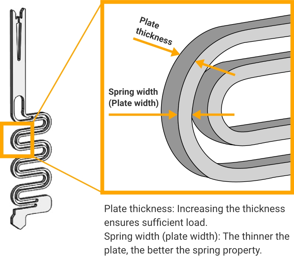
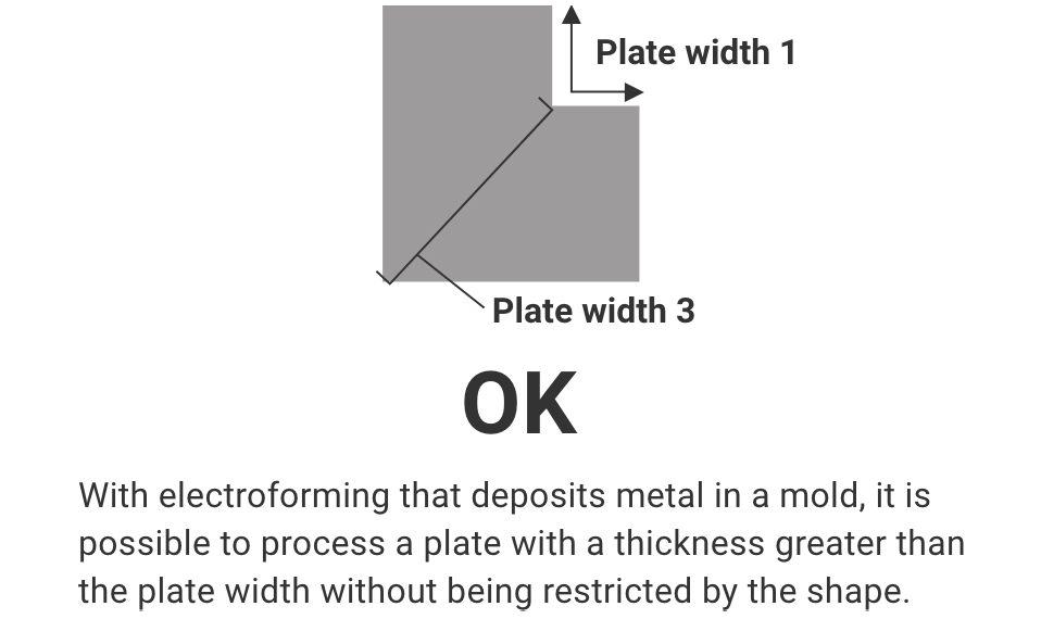
In sheet metal processing, a factor that greatly affects processing is the thickness of the material. Although there is no problem with wider plate widths, the thicker the metal plate, the more difficult it is to bend and hollow out, the less stable it is, and it is more likely for quality to vary. In press working and etching, processing under the condition of plate width ≤ plate thickness is difficult, and processing at a ratio of plate thickness : plate width = 1:1 is considered to be the limit. On the other hand, electroforming can produce thicknesses up to the ratio of plate thickness : plate width = 3:1. If the plate width is thick, the spring will not return to its original state due to plastic deformation, so the thinner the plate width, the better the spring property. However, if the pin is thin, a sufficient load cannot be secured and the contact pressure becomes low which will increase the resistance of the pin and make it difficult to carry a large current. Therefore, increasing the plate thickness makes it possible to achieve a higher load while ensuring sufficient spring property.
OMRON’s EFC process technology reproduces this complex shape with an extremely small pin size while achieving a plate thickness three times the width of the plate, thereby providing customers with high-performance testing pins.
| Press working | Electroforming process |
|---|---|
For punching, the limit is up to a ratio of plate thickness : plate width = 1:1.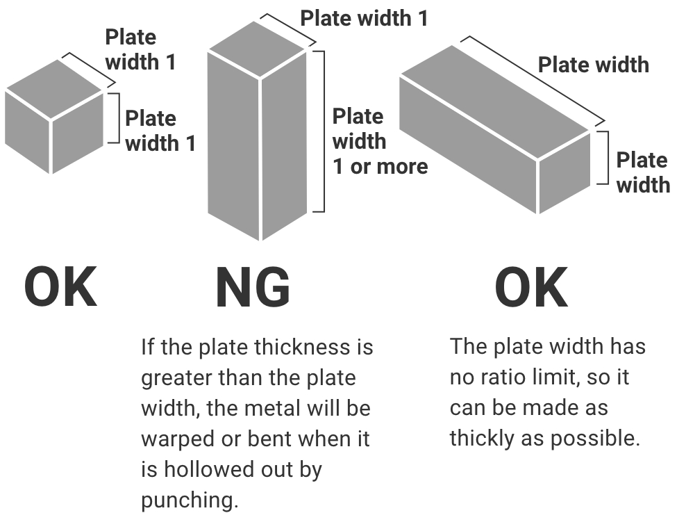 |
The ratio of thickness : width up to 3:1!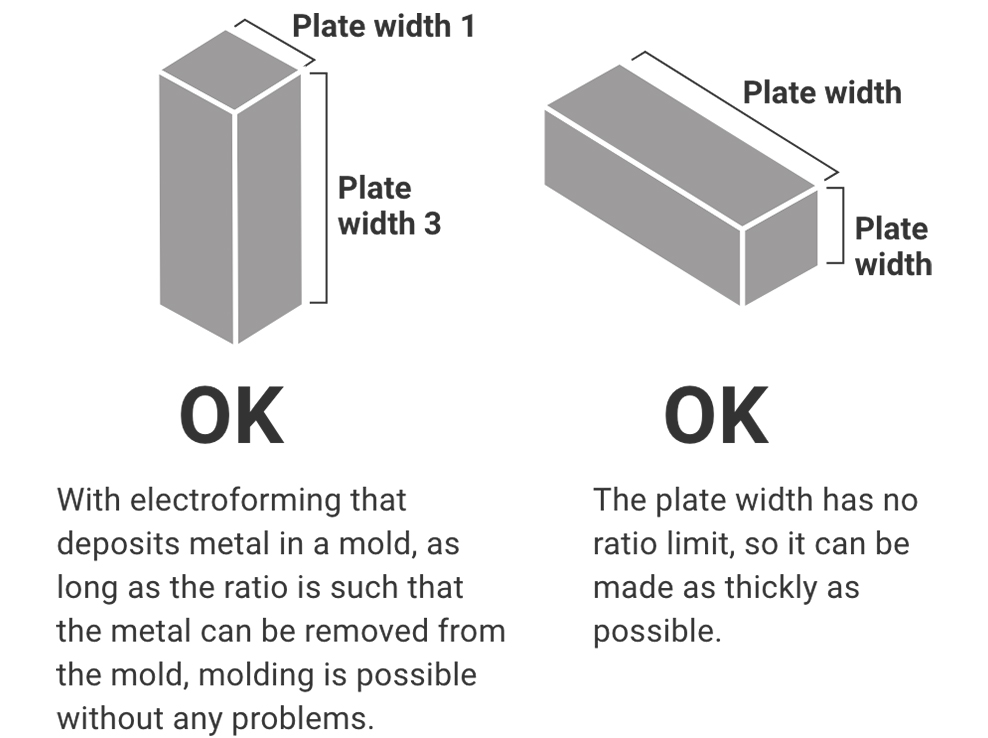 |
When bent with a press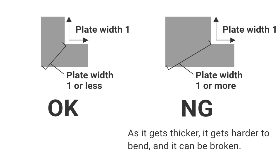 |
 |

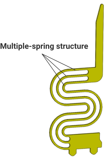
One of the strengths of the EFC process technology, a manufacturing method that deposits metal in a mold, is its ability to create unique shapes that are difficult to achieve with press working, etching, wire processing, and other methods. For example, by connecting multiple springs, it is possible to realize a multiple-spring structure that creates a conduction area that allows a large current to flow while ensuring the spring property. Such creative designs allow us to work with our customers to create high-performance testing pins in configurations tailored to each customer’s application.

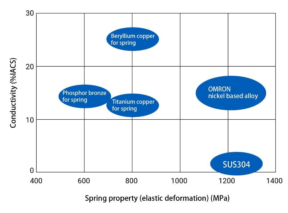
We are also particular about materials when using the EFC process technology, which often involves complex shape formation. We use OMRON’s original nickel-based alloy that has all the advantages of high spring property, high conductivity, and high hardness (long operating life), which can be processed only with the EFC process technology. It is possible to process pins with mechanical properties equivalent to SUS, electrical properties equivalent to copper alloys, and hardness specifications higher than beryllium copper.
*Patent No. 5077479