Applications: Relay Technology - MOS FET Relays (No Movable Contacts)
- Basics
- Technology
- General Application
- Glossary
MOS FET Relay Selection Method
How to select a MOS FET relay
Select a MOS FET relay by following the procedure below:
- (1) Voltage (output side)
- (2) Current (output side)
- Note: For AC, check the peak value
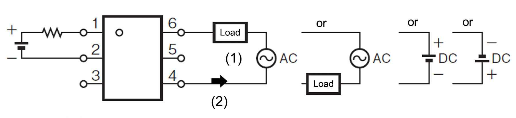
- (3) Contact type selection (SPST-NO (1a) or SPST-NC (1b))
| Input current | SPST-NO (1a) | SPST-NC (1b) |
|---|---|---|
| Not energized | 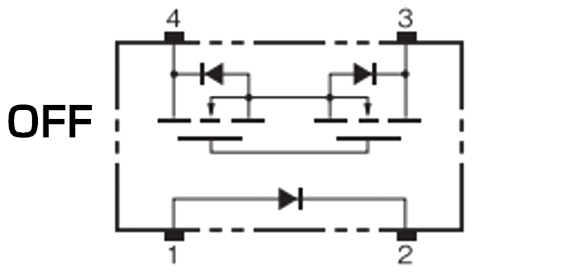 |
 |
| Energized | 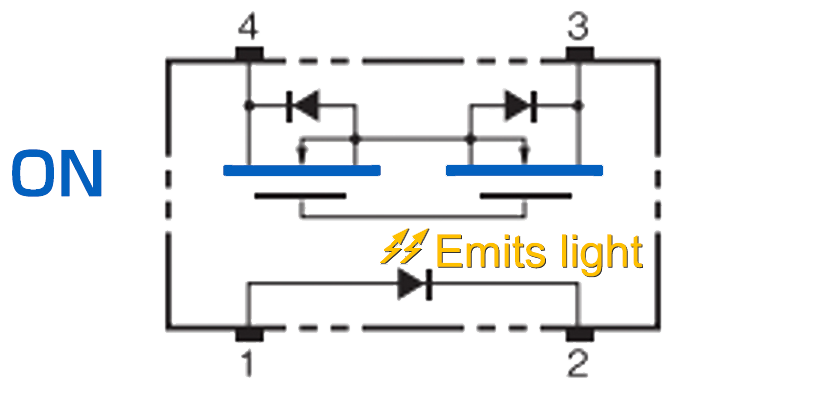 |
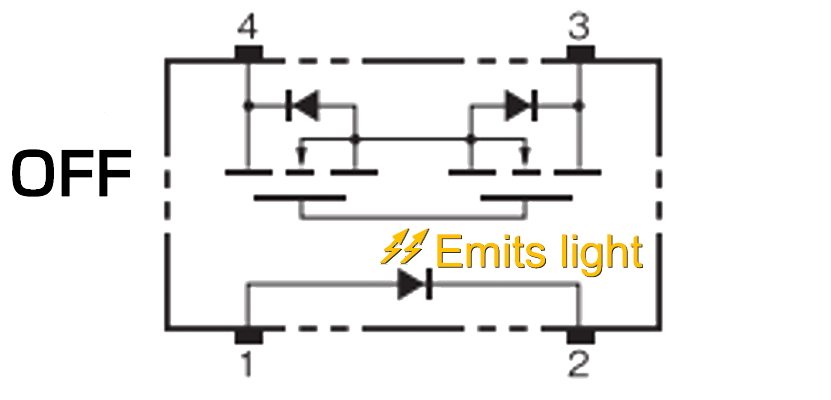 |
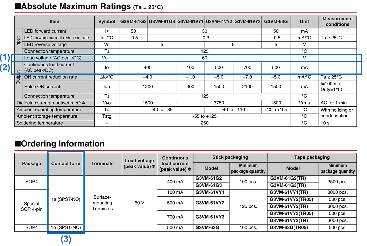
When selecting a MOS FET relay from the datasheet
When selecting a MOS FET relay from the datasheet based on the following selection criteria, check each item indicated by a blue frame.
- [Example of Selection Criteria]
- (1) Voltage (output side): 60 VDC
- (2) Current (output side): 500 mA
- (3) Contact type: SPST-NO (1a)
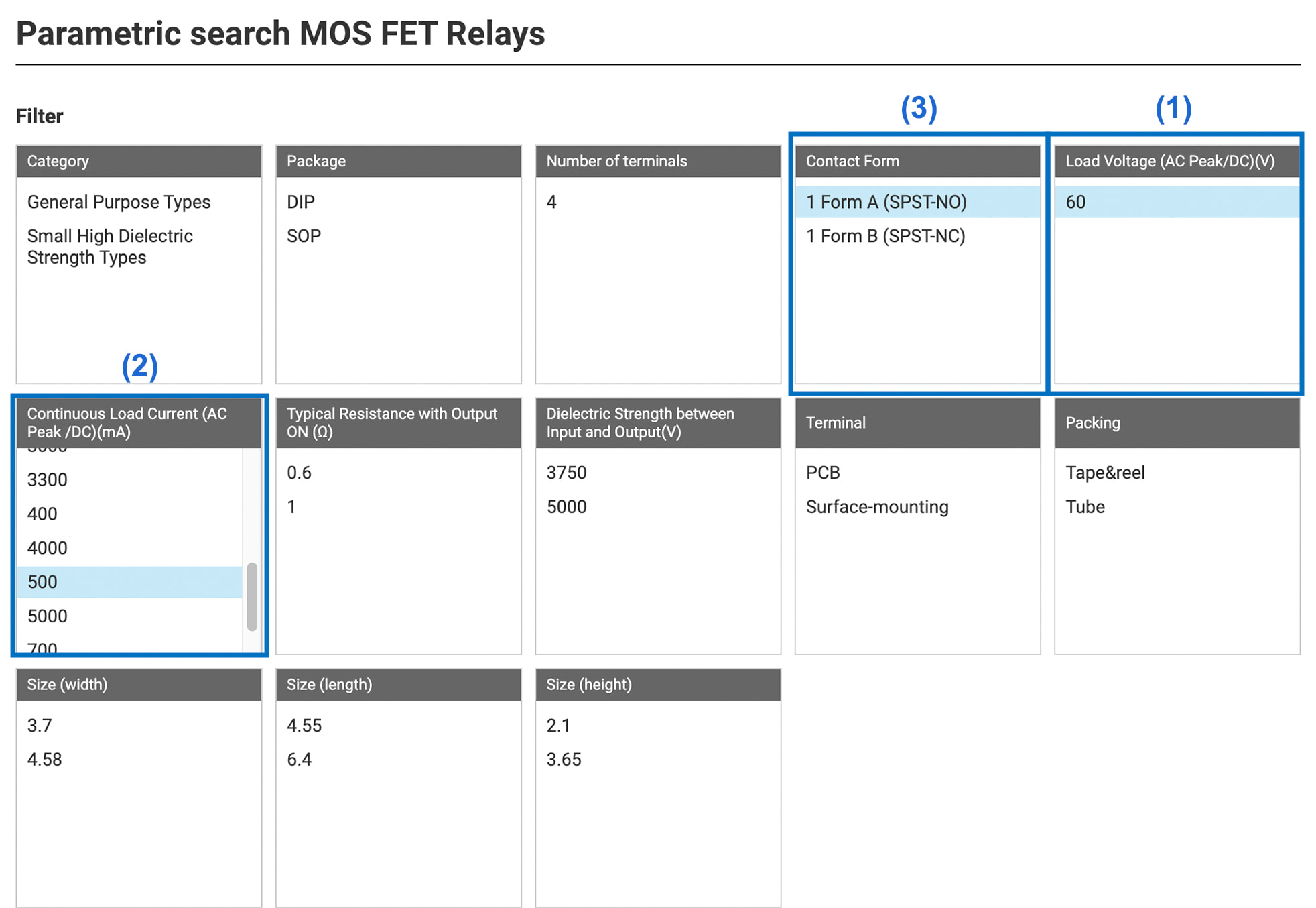
When selecting a MOS FET relay by parametric search
There are many MOS FET relays with the same external size but different specifications, so when using parametric search, we recommend that you use the method to narrow down the above three items (1), (2) and (3).
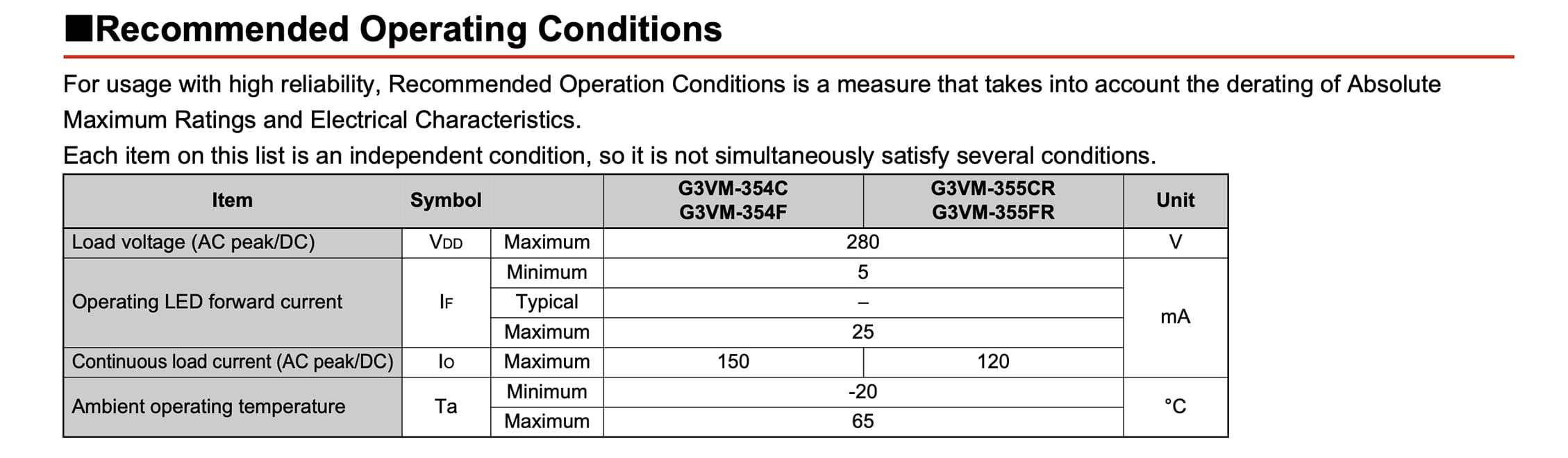
Recommended Operating Conditions for MOS FET Relays
For the design value of the operating current of the MOS FET relay, the circuit must be designed within the range of the "Recommended Operating Conditions" described in the datasheet.
For those who want to design circuits in detail
MOS FET relays have no physical contacts and are essentially semi-permanent. Therefore, the life expectancy is predicted by estimating the light intensity of the LEDs.
The light intensity of LEDs varies depending on various factors. The larger the current value, the stronger the light intensity. After many years of use, the light will gradually become weaker due to deterioration. Therefore, in order to ensure long use, the amount of light emitted during aging must be taken into consideration. Furthermore, a higher temperature environment requires a higher voltage to drive the MOS FET, thus requiring larger currents than in a normal temperature environment. MOS FET relays cannot carry larger currents than the rated value. If these factors are not properly incorporated into the design, equipment failure will result.
- Influence of ambient temperature environment
- LED aging
A more detailed explanation is provided in "Current Value Concept for Input-side Power Supply Design".
MOS FET Relay Circuit Examples
Shown below are examples of input- and output-side circuits using a MOS FET relay.
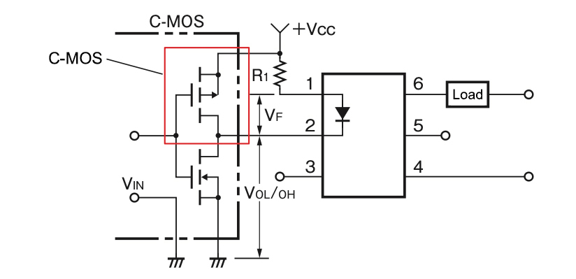
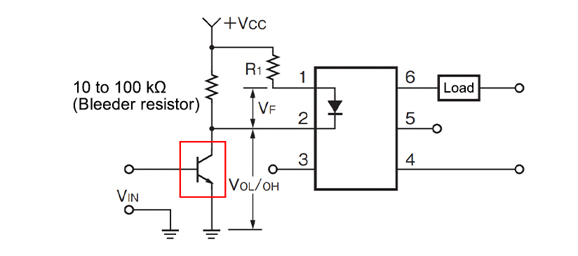
Circuit examples of MOS FET relay (input side)
Surge protection circuit (input side)
The following circuits are typical examples:
Drive circuit examples
C-MOS
Transistor
Circuit examples of MOS FET relay (output side)
Using external diode to absorb energy
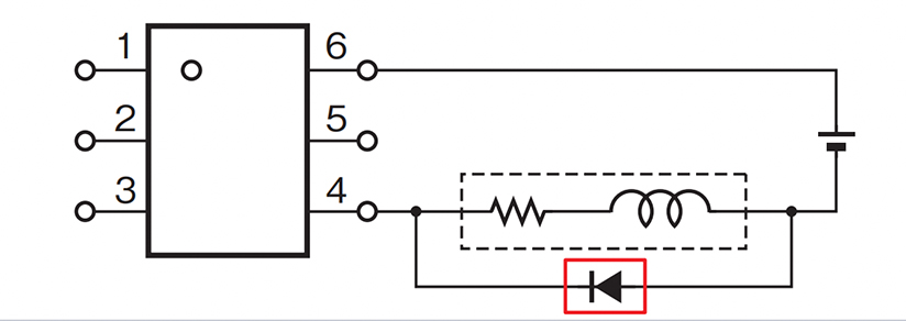
Selection guideline:
Use a diode with a reverse withstand voltage of at least 10 times the circuit voltage and a forward current larger than the load current.
Using snubber circuit to absorb energy
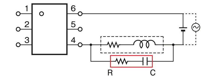
Selection guideline:
C and R as a guide:
C = 0.5 to 1 (μF) for a contact current of 1A, and
R = 0.5 to 1 (Ω) for a contact voltage of 1V.
The above values vary depending on the nature of the load and variations in characteristics. The capacitor suppresses the spark discharge of current when the contact is open, while the resistor limits the inrush current when the contact is closed again. These roles of capacitor and resistor must be considered when determining the ideal capacitance and resistance values through experimentation. Use a capacitor that can withstand voltage of between 200 and 300V. For AC circuit, use non-polarized capacitor (a condenser exclusively for AC). When there is a problem to interrupt the arcs between the contacts at high DC voltage, in some cases, it is more effective in connecting the capacitor and resistor across the contacts rather than across the load. However, a test should be performed on the actual equipment to substantiate this.
Using varistor to reduce overvoltage
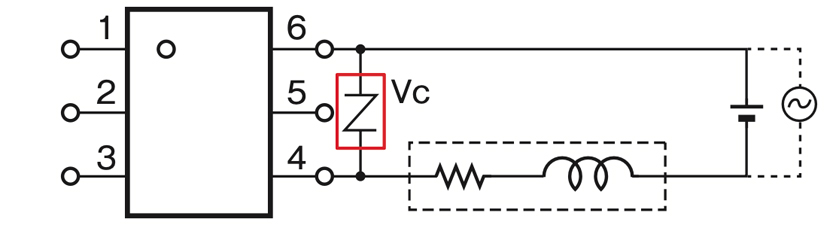
Selection guideline:
The cutoff voltage (Vc) of the varistor must satisfy the following conditions. For AC, it must be multiplied by ![]()
Vc > (supply voltage x 1.5)
If Vc is set too high, the varistor may not be able to reduce high voltage as it should and result to less effect.
Remarks:
- Protection devices may delay the recovery (breaking time) on the load side. Make sure to perform a test under actual load condition to check the performance before actual use.
- Protection devices, including diode, snubber (C-R) and varistor must be installed as close as possible to either the load or MOS FET. Longer distance may affect the performance of the protection device.
Selection of varistor
■Connect varistor across the output side terminals.
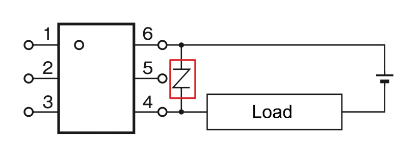
■How to select
The voltage of the varistor must not exceed the load voltage (VOFF) of MOS FET relay.
- For ESD protection, multilayer chip varistor is most commonly used.
- Please refer to the following table of varistor guidance when using commercial AC power supply.
Varistor guidance
| Supply voltage | Recommended varistor voltage | Absolute max. rated VOFF | Surge withstand capability |
|---|---|---|---|
| 100 VAC line | 220 - 270 V | 400 - 600 V | 1000A or higher |
| 200 VAC line | 430 - 470 V | 600 V | 1000A or higher |
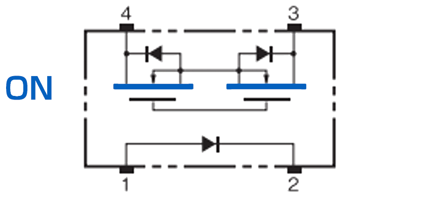
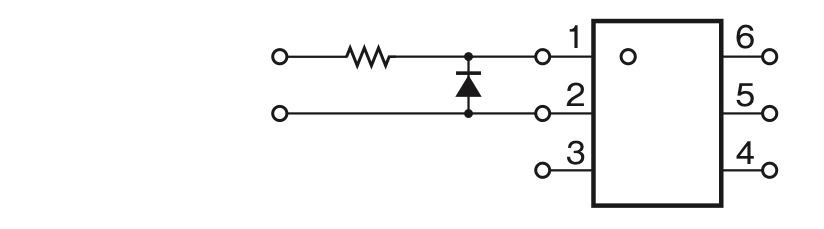
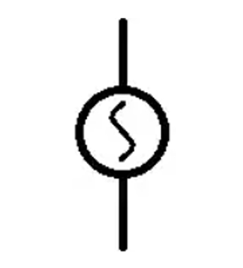
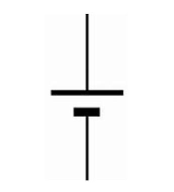
Schematic symbols found in non-contact relay circuit diagrams
The following symbols are used in the circuit diagram of a non-contact relay.
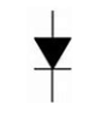
Parasitic diode (body diode)
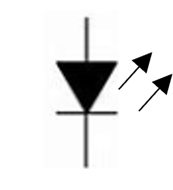
Light emitting diode
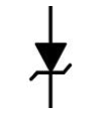
Zener diode
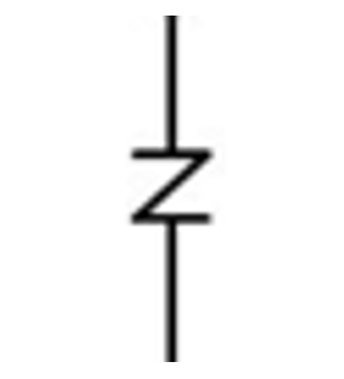
Varistor
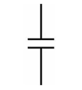
Capacitor
AC power supply
DC power supply
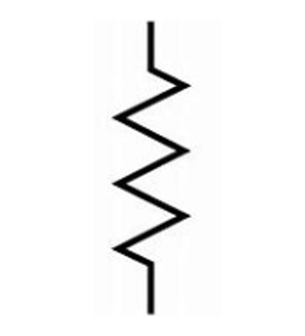
Resistor
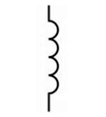
Coil
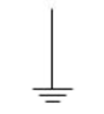
Ground electrode
Note: Old JIS electric circuit symbols are used.
- Basics
- Technology
- General Application
- Glossary
Click here for the relay product lineup