Relay Basics:
Relay Technology – MOS FET Relays
(No Movable Contacts)
- Basics
- Technology
- General Application
- Glossary
Current value in input power supply design
Table of Contents
Concerns when designing input-side power supply
Mechanical relays and MOS FET relays have different advantages. Due to the need for the advantages of MOS FET relays, such as compact size, long life, and quiet operation, there may be cases where customers want to switch from their current mechanical relays to MOS FET relays.
However, since mechanical relays and MOS FET relays have completely different product structures, the points to be considered when designing them are naturally different.
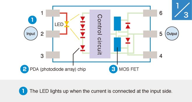
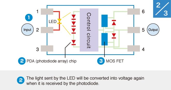
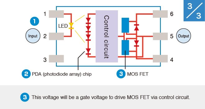
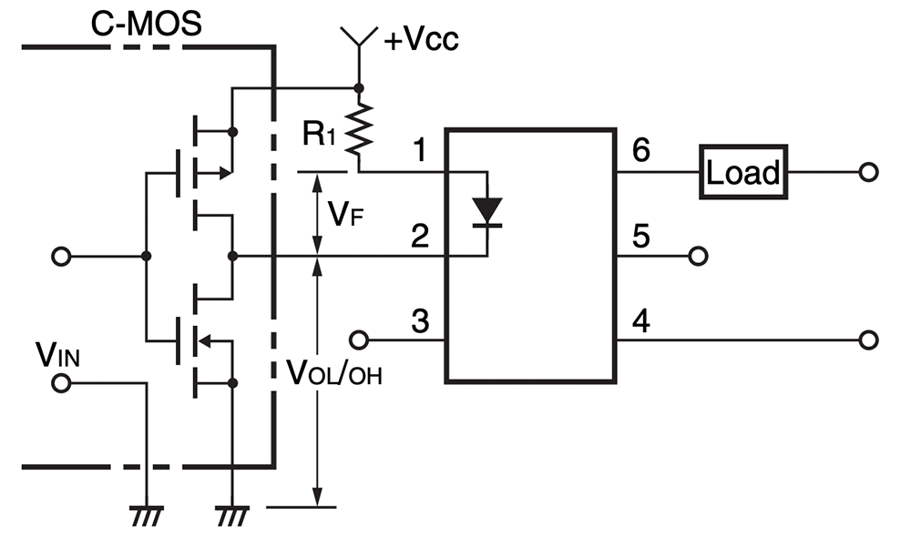
Mechanical relays are driven by applying voltage to the coil, but MOS FET relays are current driven. Unlike mechanical relays, MOS FET relays are structured in such a way that an LED on the input side emits light when current is applied, and a photodiode array (PDA) on the output side generates electricity according to the amount of light received and is driven by applying voltage to the MOS FET relay. Therefore, an important design issue is how much current to apply to the LED to drive the MOS FET relay.
The light intensity of LEDs varies depending on various factors. The higher the current value, the stronger the light intensity. After many years of use, the LED light gradually weakens due to degradation. Therefore, in order to ensure long use, the amount of light emitted over time must also be taken into consideration. Furthermore, if the temperature is higher than normal, the voltage required to drive the MOS FET relay is higher, requiring a larger current than at normal temperature.
MOS FET relays cannot carry larger current than the rated value. Failure to properly incorporate these factors into the design will result in equipment failure.
Many customers probably puzzled over the design of this input-side power supply.
This is because the design considerations are different from those for mechanical relays due to the use of LEDs.
There are two points.
- Influence of ambient temperature environment
- LED aging degradation
This issue introduces what our customers most frequently consult us about: the concept of current value when designing the input-side power supply for MOS FET relays.
For MOS FET relay troubleshooting, please use The Solutions.
Review of MOS FET relays
First, let's review the structure and operating principle of MOS FET relays.
MOS FET relays are devices that combine semiconductor elements (LEDs, PDAs, MOS FET chips) to realize relay functions.
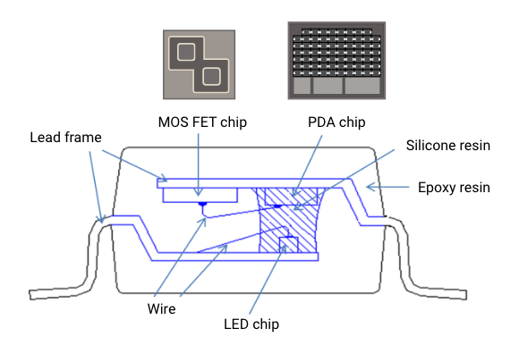
As mentioned above, a MOS FET relay operates by applying current to the input to cause the LED to emit light, and by converting the light into a voltage with a PDA to drive the MOS FET relay that is the output element. In other words, it is necessary to design the power supply on the input side so that an appropriate current can be applied to the LED and the PDA can continue to receive light. The two key points are as follows.
* Recommended conditions for LED forward current on the input side are described in our data sheet. Please use it as a reference.
Slide the image to see the operating principle.

*Point (1): LED aging degradation*
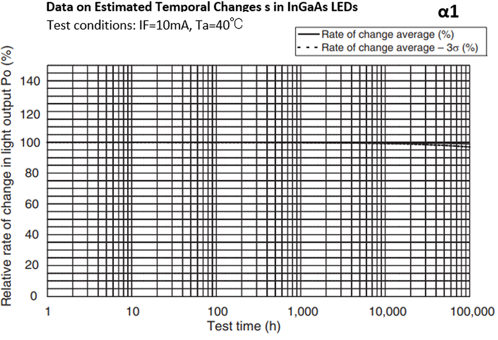
* Corresponds to α1 in the calculation formula for the input- side current value.
LEDs gradually degrade over time. The higher the input-side current, the faster the degradation rate, so the input-side current value should be designed with this in mind. In addition, the type of LEDs mounted on each MOS FET relay product differs, and at the same time, the aging degradation rate also differs. We have published information on LEDs, so please use this information as a basis for your design.
Click here for life expectancy of OMRON's various LEDs
There may be some people who design based on a high current value, thinking that selecting a high current within the range of the rated current or lower will be fine because there will be no problem in operation. However, in that case, there will be a disadvantage. The current on the input side flows almost directly to the LED, which degrades the LED and causes a decrease in the amount of light emitted. As a result, there may be cases where the MOS FET relay does not operate normally. In the worst case, the MOS FET relay may stop working due to the failure of the LED. Therefore, in order to ensure normal operation and long-term use, the relay must be designed to allow the appropriate current to flow so that the LED can emit light at an appropriate intensity.
* Recommended conditions for LED forward current on the input side are described in our data sheet. Please use it as a reference.
Point (2): Consideration of ambient operating temperature*
* Corresponds to α2 in the calculation formula for the input- side current value.
The degradation rate of the LED is also accelerated by the operating temperature conditions under which the LED is used. The higher the operating temperature, the faster the degradation rate, so the input-side current value should be designed with this in mind.
* Refer to the datasheet on each product page for ambient operating temperature conditions.
Point (3): Other considerations*
* Corresponds to α3 in the calculation formula for the input- side current value.
Another thing, which is not limited to our devices, is that the design is likely to be made with safety in mind, depending on the customer's approach to quality. It would be appreciated if this point could also be reflected in the design of the input-side current value.
Input-side current value calculation formula
Considering the three points, the value can be obtained for the design of the input-side current value as follows:
- Operating LED forward current design value = IFT x α1 x α2 (x α3)
- IFT: Trigger LED forward current ... Based on the maximum standard value in the catalog.
- α1: LED aging rate ... Differs by model (the type of LED used).
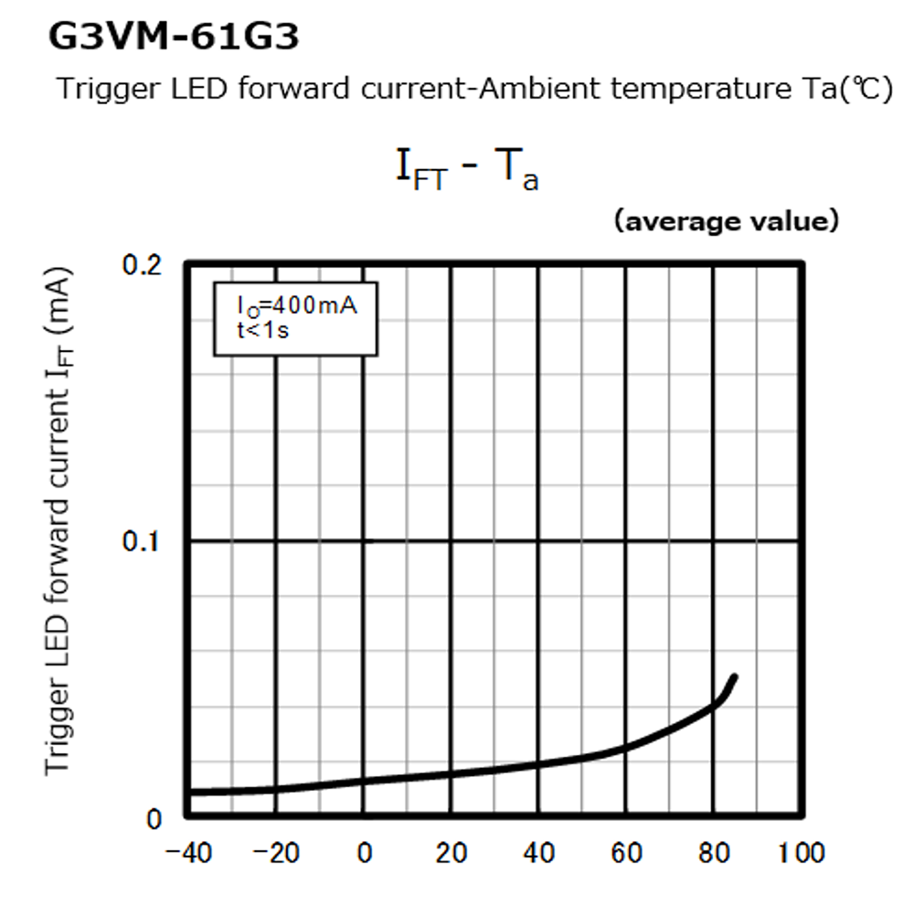
Refer to "● Estimated Life" in Common Precautions (PDF). - α2: IFT ambient temperature change ... from the "Trigger LED forward current vs. Ambient temperature" graph in the catalog.
- α3: Safety factor ... Variations and degradation of power supplies, and others.
For example, assuming that G3VM-61G3 is used at a maximum ambient temperature of 85°C
- IFT: 0.2 mA (maximum rated value, at 25°C)
- α1: Set for 95% (5% reduction) after 100,000 hours of useful life based on the data of LED's expected life expectancy → 1÷0.95=1.05
(When room temperature rises, aging accelerates. Therefore the aging rate increases more at 85°C compared to the data at 40°C. However, the rate will slow down if used under the condition that is lower than the IF condition of 10 mA. 95% is set considering this point.) - α2Set the aging rate based on the values of room temperature at 20°C and 85°C referring to the Graph: Trigger LED forward current vs. Ambient temperature
→ 0.05 mA÷0.02 mA=2.5
The calculation formula is as follows:
Design value of operating LED forward current = 0.2mA x 1.05 x 2.5 (x α3) = approx. 0.53mA (x α3)
Summary
Is the above explanation clear?
When designing an LED input power supply, please consider (1) the effects of ambient temperature and (2) the effects of LED aging degradation.
Other precautions for input-side power supply design are also described in the following "Common Precautions".
Common Precautions for All MOS FET Relays
Other related contents


- Basics
- Technology
- General Application
- Glossary
Click here for the relay product lineup