
Photomicrosensor Basics: Design Ⅱ
(Design of Systems Incorporating Photomicrosensors)
(1) Phototransistor OutputCharacteristics of the Detector
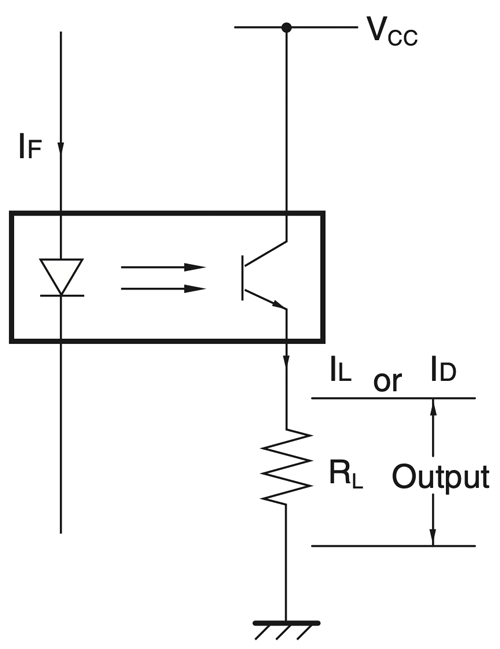
Figure 7. Measuring Circuit
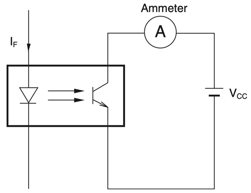
The changes in the current flow of the output detector, with and without an optical input from the LED, are important. Figure 7 shows a circuit used to measure how much current flows through the phototransistor with an appropriate forward current (IF). The following explains the ideal condition of no ambient light(i.e., 0 ℓx).
When there is no LED forward current (IF) flowing or the optical beam emitted from the LED is completely intercepted by an opaque object, the ammeter indicates several nanoamperes due to a current leaking from the phototransistor. This current is called the dark current (ID). When the (IF) flows with no object intercepting the optical beam, the ammeter indicates several milliamperes. This current is called the light current (IL).
- When the optical beam to the phototransistor is interrupted・・・Dark current (ID): 10-9 A
- When optical beam to the phototransistor is not interrupted・・・Light current (IL): 10-3 A
The difference(ratio) between (ID) and (ID) is about 106 times. This difference (ratio) in current through the phototransistor output element can be applied to the sensing of a variety of objects.
In actual operation, there is generally a small amount of ambient light located close to the Photomicrosensors (photointerrupters). Therefore, a small amount of current will flow into the phototransistor in addition to the dark current (ID), because of the ambient light. This occurs even when the LED’s optical beam is not incident on the output detector.
In the case of a reflective Photomicrosensor, the dark current flows when there is no sensed object. However, due to the structure of the Photomicrosensor, a small portion of the LED’s optical beam also reaches the phototransistor (the output element) due to reflections within the sensor’s housing. Subsequently the dark current and the other additional current will flow into the phototransistor. The other additional current generated by the impact of the inside reflections is called leakage current (ILEAK). The (ID) of the phototransistor is several nanoamperes. On the other hand, the lLEAK is several hundred nanoamperes.
Figure 8. Dark Current vs. Ambient Temperature
Characteristics (Typical) EE-SX1081
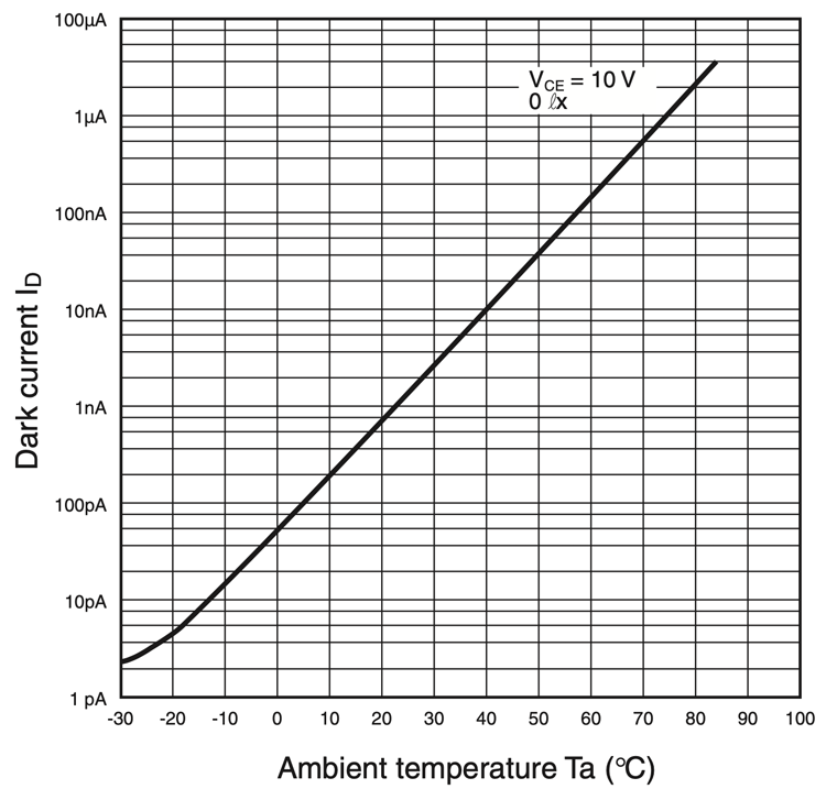
The dark current (ID) of the phototransistor has temperature dependencies, which must not be ignored in the circuit design for the Photomicrosensor (photointerrupter). The (ID) will considerably increase when the ambient temperature increases. Figure 8 shows the dark current temperature dependency for the EE-SX1081. Pay attention to the dark current (ID) when Photomicrosensors (photointerrupters) are operated in high temperature.
The light current (IL) of the phototransistor also increases when the ambient temperature increases. As shown in Figure 9, the amount of light emitting from the LED decreases due to the temperature dependency of the LED. An increase in the output’s light current is offset by a decrease of the amount of light emitting from the LED. Consequently, the change of the light current at the Photomicrosensor’s output, due to a change in the ambient temperature, is comparatively small.
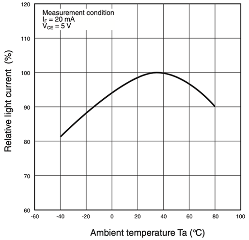
Refer to Figure 10 for the light current temperature dependency of EE-SX1081. The temperature dependency curve shown in Figure 10 is only a typical example. The actual light current’s fluctuation caused by temperature changes varies for each Photomicrosensor (photointerrupter); it is different from sensor to sensor and lot to lot. This means that designing any circuit to account for temperature compensation is difficult.
Figure 9. LED and Phototransistor Temperature Characteristics (Typical)
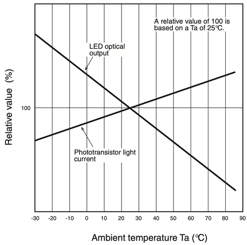
Figure 10. Relative Light Current vs. Ambient (Typical) Temperature Characteristics
EE-SX1081
Changes in Characteristics
The following explains the important points required for the designing of systems incorporating Photomicrosensors (photointerrupters) by considering worst-case design technique. Worst-case design technique is a method to design systems so that the Photomicrosensors (photointerrupter) will operate properly even if the various input and output characteristics of the Photomicrosensors (photointerrupters) are functionally at their extreme limits.
For example, the minimum value for the light current (IL), the maximum value for the dark current and the additional current (ID + α) caused by internal reflections or ambient light, are typically the worst-case values during the operation. The minimum ratio between a current with a sensed object and a current without any object can be predicted if the above worst-case values are considered. The goal is to make the ratio as large as possible for these conditions, in order to allow the output to change states from ‘Off’ to ‘On’, with no ambiguity from one sensor to the next or from one lot to the next.
The lower limit of the (IL) and the upper limit of the (ID) are specified in the datasheet. Table 1 shows these values for typical Photomicrosensor models.
Table 1. Rated Dark Current (ID) and Light Current (IL) Values
| Model | Upper limit (ID) | Lower limit (IL) | Condition |
|---|---|---|---|
| EE-SG3 | 200 nA | 2 mA | IF = 15mA |
| EE-SX1081, EE-SX1035 EE-SX1096(-W11), etc. | 200 nA | 0.5 mA | IF = 20mA |
| EE-SY110 EE-SF5(-B), etc. | 200 nA | 0.2 mA | IF = 20 mA (see note) |
| Conditions | VCE = 10V, 0ℓx Ta = 25°C | VCE = 10V Ta = 25°C | --- |
Note: These values were measured under the standard conditions specified by OMRON for the corresponding Photomicrosensors.
Within an actual system design, not only these values but also the following factors must be considered to determine the upper limit of the dark current, the additional current (ID + α), and the lower limit of the light current (IL).
The following factors increase the ID and the additional current when the optical beam to the detector is intercepted;
The following factors decrease the IL when the optical beam to the detector is not intercepted;
- Temperature change
- Aging change (Degradation of LED - - causing a reduction in the amount of light emitted, over time.)
Figure 8. Dark Current vs. Ambient Temperature Characteristics (Typical)
EE-SX1081
Figure 11. Dark Current Imposed Voltage Dependency (Typical)
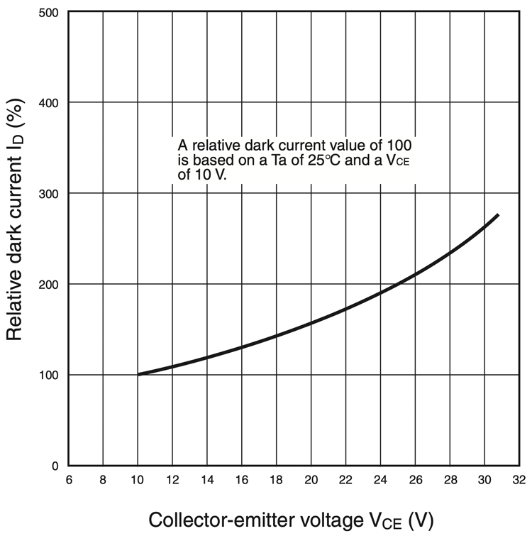
Table 2 shows the increases to (ID + α) and the decreases to (ID) that are caused by the above factors.
For example, if the EE-SX1081 is operated at a Ta of 60°C maximum and a VCC of 10 VDC for approximately 50,000 hours, the (ID) upper limit value of EE-SX1081 will be calculated 4 µA (20 times the value of 200 nA at 25 °C).
And the (IL) lower limit value will be calculated to be 0.25 mA (1/2 of 0.5 mA at 25°C). Considering 1/2 the minimum rated (IL) at 25°C when designing the circuit, accounts for LED degradation over time.
Table 2. Dependency of Detector Elements on Various Factors
| Elements | Phototransistor | |
|---|---|---|
| Dark current ID | External light interference | To be checked using experiment |
| Temperature rise | Increased by approximately 10 times with a temperature rise of 25°C. | |
| Supply voltage | See Figure 11. | |
| Light current IL | Temperature change | Approximately -20% to 10% |
| Aging change (20,000 to 50,000 hours) Note: For an infrared LED. | Decreased to approximately one-half of the initial value considering the temperature changes of the element. | |
Table 3 shows the estimated worst-case values for typical models of Photomicrosensors. These values should be used when designing systems. The dispersion of the characteristics of the Photomicrosensors must be also considered, which is explained in detail later.
Regarding reflective Photomicrosensors: The light currents (IL) in our datasheets were specified using our standard operating conditions (i.e., sensing object: white paper, etc.). Make sure that the light current (IL) of any reflective Photomicrosensor greatly varies with regards to sensed object and sensing distance in your actual applications. (Ensure that the ratio between object / mark sensed and object / mark not sensed is as large as possible under all conditions. Otherwise, the output will appear to be non-functioning.)
Table 3. Estimated Worst Values of a Variety of Photomicrosensors
| Model | Estimated worst value (ID) | Estimated worst value (IL) | Condition |
|---|---|---|---|
| EE-SG3 | 4 μA | 1 mA | IF = 15 mA |
| EE-SX1081, EE-SX1035 EE-SX1340, EE-SX1096(-W11), etc. | 4 μA | 0.25 mA | IF = 20 mA |
| EE-SY110 EE-SF5(-B), etc. | 4 μA | 0.1 mA | IF = 20 mA (see note) |
| Conditions | VCE = 10V, 0ℓx Ta = 60°C | VCE = 10V, Operating hours = 50,000 to 100,000 hrs Ta = Topr | --- |
Note: These values were measured under the standard conditions specified by OMRON for the corresponding Photomicrosensors with an Infrared LED.
Design of Basic Circuitry
In the design stage, as explained above, it is necessary to understand the important characteristics and what factors those characteristics are based on; how those characteristics change, and how changed characteristics should be used. The following section describes concrete design methods and explains main design points.
The first point to note is how the flowing currents (i.e., IL and ID) of the phototransistor must be processed to obtain the output of the Photomicrosensor (photointerrupter).
Figure 12 shows the basic circuit for a Photomicrosensor. As expressed in the figure;
- The light current (IL) will flow into the resistor (RL) when the phototransistor receives an optical input.
- The dark current and the additional current (ID + α) of the phototransistor will flow into the resistor (RL) when the phototransistor does not receive any optical input.
Therefore, if the phototransistor receives an optical input, the output voltage imposed on the resistor (RL) will be obtained from the following:
IL x RL
If the phototransistor does not receive any optical input, the output voltage imposed on the resistor (RL) will be obtained from the following:
(ID +α) x RL
Be sure to apply the estimated worst-case values mentioned earlier for the light current (IL) and dark current (ID) and the additional current described in the following explanation.
The output voltage of the phototransistor is obtained by simply connecting the resistor (RL) to the phototransistor. For example, to obtain an output of 4 V minimum from the phototransistor when it is ON and an output of 1 V maximum when the phototransistor is OFF, assume the estimated worst-case value for the light current (IL) is 0.25 mA and the estimated worst-case value for the current (ID +α) is 0.01 mA;
Figure 12. Basic Circutt
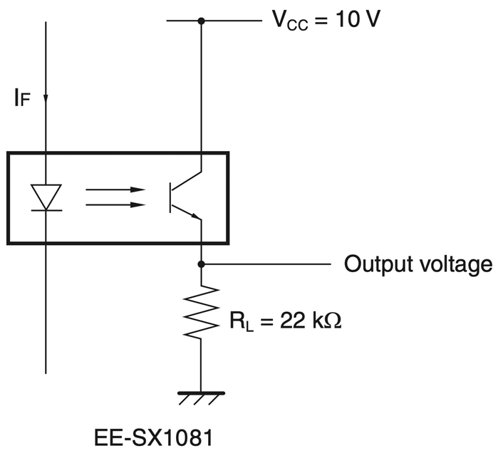
As shown in Figure 13, if the resistance of the resistor (RL) is approximately 22 kΩ;
- An output of 5.5 V (0.25 mA x 22 kΩ) will be obtained when the phototransistor is ON.
- An output of 0.22 V (0.01 mA x 22 kΩ) will be obtained when the phototransistor is OFF.
These conditions meet the criteria of 4 V minimum when ON and 1 V maximum when OFF.
Practically, the actual output voltage will be more than 5.5 V when the phototransistor is ON and less than 0.22 V when the phototransistor is OFF, because the above voltage calculations are based on the estimated worst-case value. The output voltages can then be used as input signals to ICs to make practical use of the Photomicrosensor (photointerrupter) .
Figure 13. Output Example (Typical)
Practical design for a circuit with a grounded Phototransistor
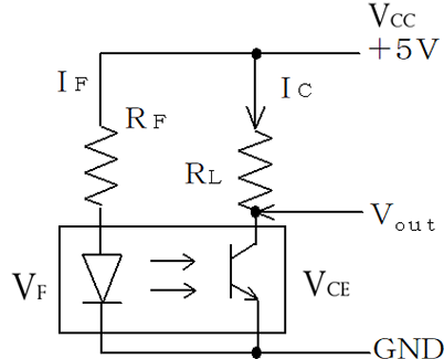
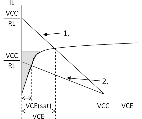
A basic circuit for a Photomicrosensor where the emitter is connected to a ground is shown in Figure 14. It is important to determine the proper resistance value of the RL in order to use the phototransistor in the saturation area according to the IL vs. VCE (voltage between collector and emitter) characteristics.
There are two formulas that are derived from the circuit shown in Figure 14: One for the input LED and one for the output phototransistor:
IF=(VCC−VF) / RF …………………(A)
VCC=IC×RL+VCE …………………(B)
Figure 14. Circuit with a grounded Phototransistor
Considering Figure 14, the calculations that allow for proper selection of RL, when RF = 220 Ω and VF = 1.2 V, are explained in the following four steps:
1. Calculate the actual LED forward current (IF)
According to formula (A), IF = (5 - 1.2) / 220 = 17 mA.
2. Obtain the minimum value of the light current (IL (MIN)) for the actual value of IF
If EE-SX1081 is used, then the datasheet shows that IL(MIN) = 0.5 mA (at IF = 20 mA). But the actual value of IF is not 20 mA. In this case, when RF = 220 Ω , IF is 17 mA.
The IL vs. VCE characteristics for this case are shown in Figure 15. In order to make the phototransistor turn ON with stability, the phototransistor should be used in the saturation region of the phototransistor.
- Out of saturation region:
According to the intersection point of the IL vs. VCE curve with the load line, VCE will be too big when RL is too small. As a result, Vout will not be low enough when the phototransistor is ON. - Within the saturation region:
If RL is determined with 50% of the IL(MIN), the phototransistor turns ON in the saturation region. This creates stable switching for a long-term operation.
Figure 15. IL vs. VCE Characteristics
Since the light current (IL) is directly proportional to the LED forward current (IF), a ratio can be created, in order to see actual value of IL that corresponds to the actual value of IF. The minimum value of IL at IF = 17 mA is obtained as follows:
Actual IL(MIN) = 0.5 mA X 17 mA / 20 mA = 0.425 mA (at actual IF = 17 mA)
3. Consider a design margin
The circuit design for Photomicrosensors (photointerrupters) must consider various changes such as an LED degradation and temperature characteristics for long-term operation. Therefore, 50% of the initial, actual IL value is recommended to be used at room temperature:
1/2 X 0.425 mA = 0.212 mA (This value accounts mainly for LED degradation over time.)
4. Determine RL
According to formula (B), RL is obtained as follows:
RL = (VCC−VCE(SAT) ) / IC ≒ VCC / IC = 5 / 0.212 = 23.8 kΩ (In this case, VCE(SAT) is considered to be negligible.) ∴ Therefore, a value of 22 kΩ is used for RL.
Design of an Applied Circuit
The following explains the functional operation of the applied circuit shown in Figure 16.
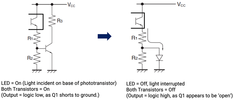
The light current (IL) of the phototransistor flows into R1 and R2 when the phototransistor receives the optical input from the LED. Part of the light current (IL) will flow into the base and emitter of Q1 when the voltage imposed on R2 exceeds the bias voltage (i.e., approximately 0.6 to 0.9 V) imposed between the base and emitter of the transistor (Q1). The light current flowing into the base turns Q1 ON. A current will flow into the collector of Q1 through R3 when Q1 is ON. Then, the electric potential of the collector will drop to a low logic level.
Figure 16. Applied Circuit
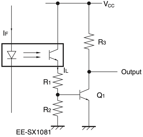
The dark current and the additional current (ID + α) of the phototransistor flow when the optical input is intercepted. The electric potential of the output of the phototransistor (i.e., (ID + α) x R2) is, however, lower than the bias voltage between the base and emitter of Q1. Therefore, no current will flow into the base of Q1 and Q1 will be OFF. The output of Q1 will be at a high level.
As shown in Figure 17, when the phototransistor is ON, the phototransistor will be seemingly short-circuited through the base and emitter of the Q1, which is equivalent to a diode. If the light current (IL) of the phototransistor is large and R1 does not exist, the light current (IL) will flow into Q1 and the collector dissipation (PC) will be excessively large. The R1 can avoid the large dissipation.
Figure 17. Equivalent Circuit
The following items are important when designing the above applied circuit:
- The voltage output (i.e., IL x R2) of the phototransistor receiving the optical input must be much higher than the bias voltage of Q1.
- The voltage output (i.e., (ID + α) x R2) of the phototransistor not receiving the optical input must be much lower than the bias voltage of Q1.
Figure 18. Applied Circuit Examples
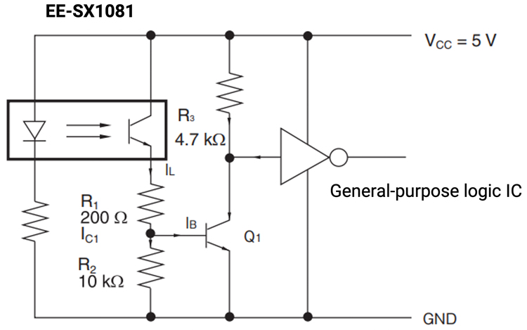
The following example explains the circuit design method for choosing values of R1 and R2 to be used in the above circuit.
(1) Calculation of R2
The resistance value of R2 should be decided using the following formula, so that the appropriate bias voltage (VBE(ON)) between the base and emitter of Q1 to turn Q1 ON will be obtained:
IC1 X R2 > VBE(ON) …………………(A)
IC1 = IL – IB
∴ (IL – IB) x R2 > VBE(ON)
∴ R2 > VBE(ON) / ( IL – IB) …………………(B)
In (A), the bias voltage (VBE(ON)) of Q1 is approximately 0.8 V and the base current (IB) of Q1 is approximately 20 µA, if Q1 is a standard transistor controlling small signals. The estimated worst-case value of the light current (IL) of EE-SX1081 is 0.25 mA according to Table 3.
Therefore, the following is obtained:
R2 > 0.8 V / ( 0.25 mA – 20 μA) = approx. 3.48 kΩ ……(C)
Since R2 must be larger than the above result, the actual resistance of R2 must be 2 to 3 times as large as the above result. In the above applied circuit example, the resistance of R2 is 10 kΩ.
(2) Verification of R2 Value
The R2 value obtained from the above turns Q1 ON. The following explains the way to confirm whether the R2 value obtained from the above equation can turns Q1 OFF as well. The condition required to turn Q1 OFF is obtained from the following:
(ID + α) x R2 < VBE(OFF) ...............................................(D)
Substitute 10 kΩ for R2, 4 µA for the dark current (ID) according to Table 3, and 10 µA for the additional current on the assumption in formula 3. The following is obtained.
(4 μA + 10 μA) × 10 kΩ = approx. 0.14 V
VBE(OFF) = 0.4 V
∴ 0.14 V < 0.4 V …………………….….…………....... (E)
According to the results of (E), it is verified that the 10 kΩ of RL is an appropriate value in the circuit shown in Figure 18.
(3) Determination of R1
As shown in Figure 17, when the phototransistor is ON, the phototransistor will be seemingly short-circuited, and if the light current (IL) of the phototransistor is large and R1 is not connected to the phototransistor, the light current will flow into Q1 and the collector dissipation of the phototransistor will be excessively large. The resistance of R1 depends on the maximum permissible collector dissipation (PC) of the phototransistor, which can be obtained from the datasheet of the Photomicrosensor. The R1 value is several hundred ohms (200 Ω in the circuit example). If the resistance of R1 is determined, the design of the circuit is complete.
This circuit connects a transistor to the output of the phototransistor, in order to amplify the output of the phototransistor, which is configured to operate as an electronic switch. This configuration improves the reliability and stability of the circuit for a Photomicrosensor.
The response speed and other performance characteristics of the applied circuit shown in Figure 16 are far superior to the basic circuit shown in Figure 12. This is because the apparent impedance (i.e., load resistance) of the Photomicrosensor (photointerrupter) is determined by R1 which is comparatively small.
Photomicrosensors that have photo IC amplifier circuits as an additional output stage are often used, because they are easy to use and make it possible to easily design circuits.
Click here for the photomicrosensor product lineup